As the new energy vehicle race enters the era of "precision millimeter" competition, a chip is rewriting the game rules of power battery management. The global analog chip giant, Adeno, continues to lead the BMS market with its profound technological accumulation and the support of series products such as ADBMS6830, ADBMS6832M, and ADBMS2950.
In 2025, ADI will once again shine the sword - launching the 24 channel multi cell battery monitor ADBMS6834, which leads the industry in voltage detection accuracy with a ± 0.003% accuracy. Its innovative dual ADC architecture improves battery balancing efficiency by 35%, and its hard core technologies such as innovative bidirectional isolated serial interface (isoSPI) and breakthrough integrated DC/DC converter make comprehensive performance leaps and reshape industry standards.
What kind of technical code is hidden behind this product, known as the "new benchmark for battery management chips"? The following text will provide you with a detailed analysis.
Firstly, let's take a look at its packaging and X-ray. The ADBMS6834 adopts a new QFN-88 packaging, which can reduce the chip area while providing good heat dissipation through the bottom metal plate. From the X-ray, it can be clearly seen that ADI still uses the previous dual die structure, where one large die is responsible for the main function of the chip, and the other small die plays a key pressing auxiliary role.
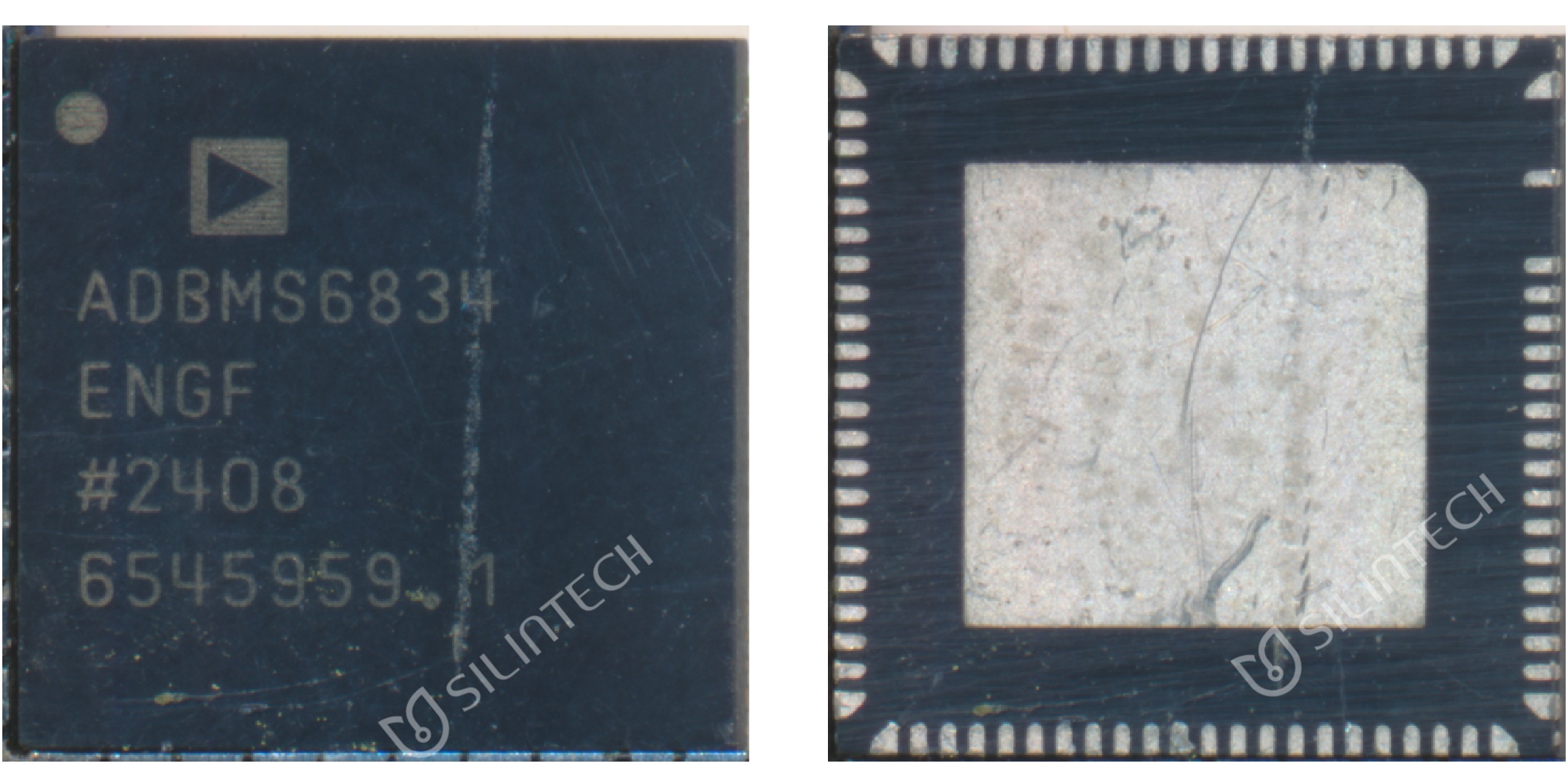 ADBMS6834 packaging diagram
 ADBMS6834 X-ray image
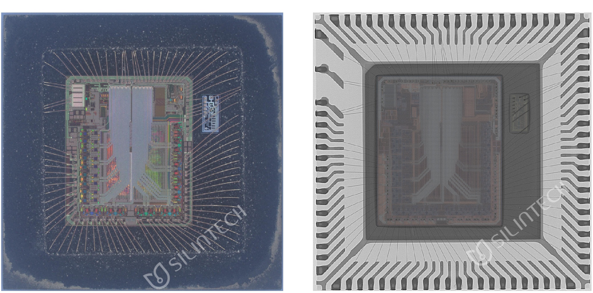
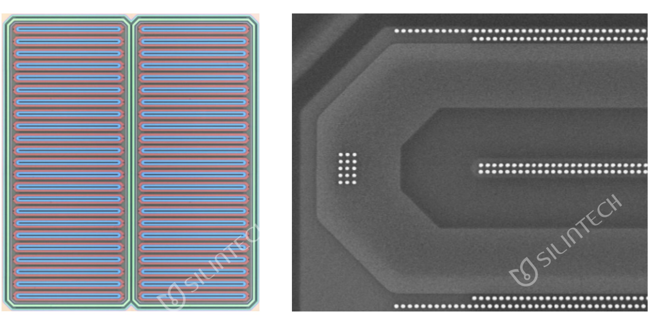
Let's focus our attention on the main die. From the analyzed floorplan and top-level circuit, it is not difficult to find that there are dual ADCs distributed around the chip for balancing circuits and synchronous detection. The VREF, which provides the reference voltage, is located in the middle of the chip and even embedded in the digital area. The reference voltage is uniformly supplied to all ADCs through 5 layers of metal lines; The signal line of the ADC is transmitted to the digital area for computation through a 6-layer metal tree structure.
The clock, voltage detection, auxiliary ADC, and storage modules are concentrated in the lower right corner of the chip; In the upper left corner, two power modules, DC/DC and LDO, as well as a serial interface module, are deployed. The DC/DC module is made in the form of a built-in power P transistor.
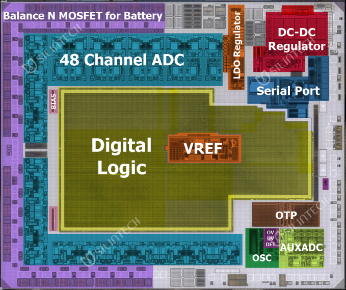
ADBMS6834 Top Floorplan
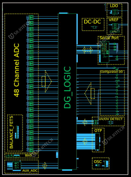
Top level schematic diagram of ADBMS6834
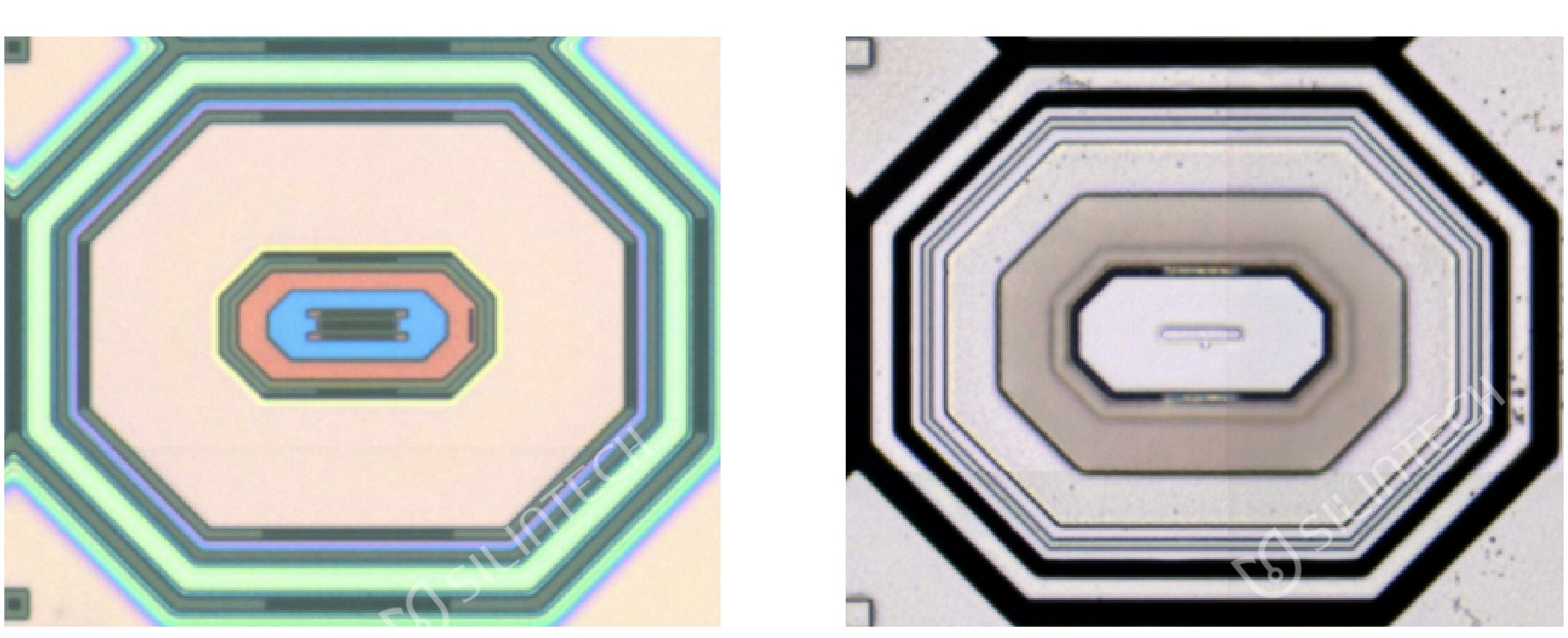
From a detailed perspective, all battery voltages in ADBMS6834 are measured simultaneously by their corresponding ADCs, and each channel is equipped with a programmable digital low-pass filter. In addition, another set of ADCs is responsible for redundant measurements to ensure compliance with safety standards. Under the working temperature and voltage range, the total measurement error (TME) is less than 3mV. The schematic diagram of a single ADC is shown below, which consists of a second-order integrator, quantizer, and analog-to-digital conversion unit.
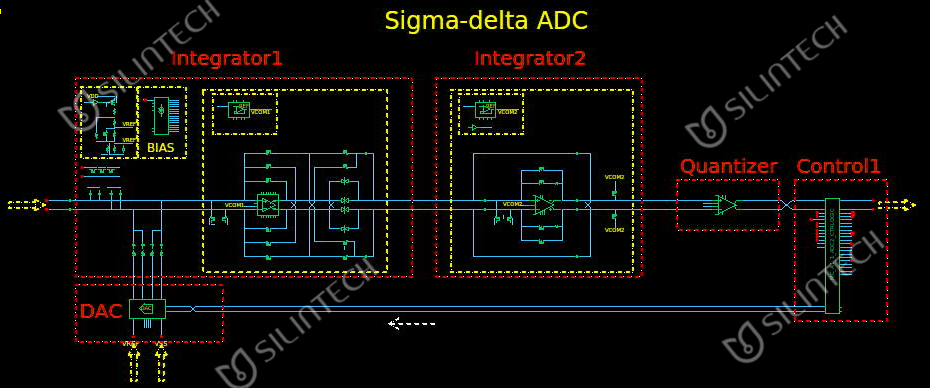
Single ADC schematic diagram
The detection unit of this chip has a flexible power supply method, which can be directly powered by the tested battery or through the built-in step-down DC-DC regulator. In DC-DC power supply mode, the power consumption of the measurement state can be significantly reduced to only 1W; while in sleep mode, the static current of the entire device is only 7uA, which can minimize the discharge of the battery pack.
From the perspective of the device, it can be clearly observed through the photos that the chip integrates various high-voltage MOS devices of different voltage levels and types, among which the device with the highest withstand voltage value is applied in the DC-DC module.
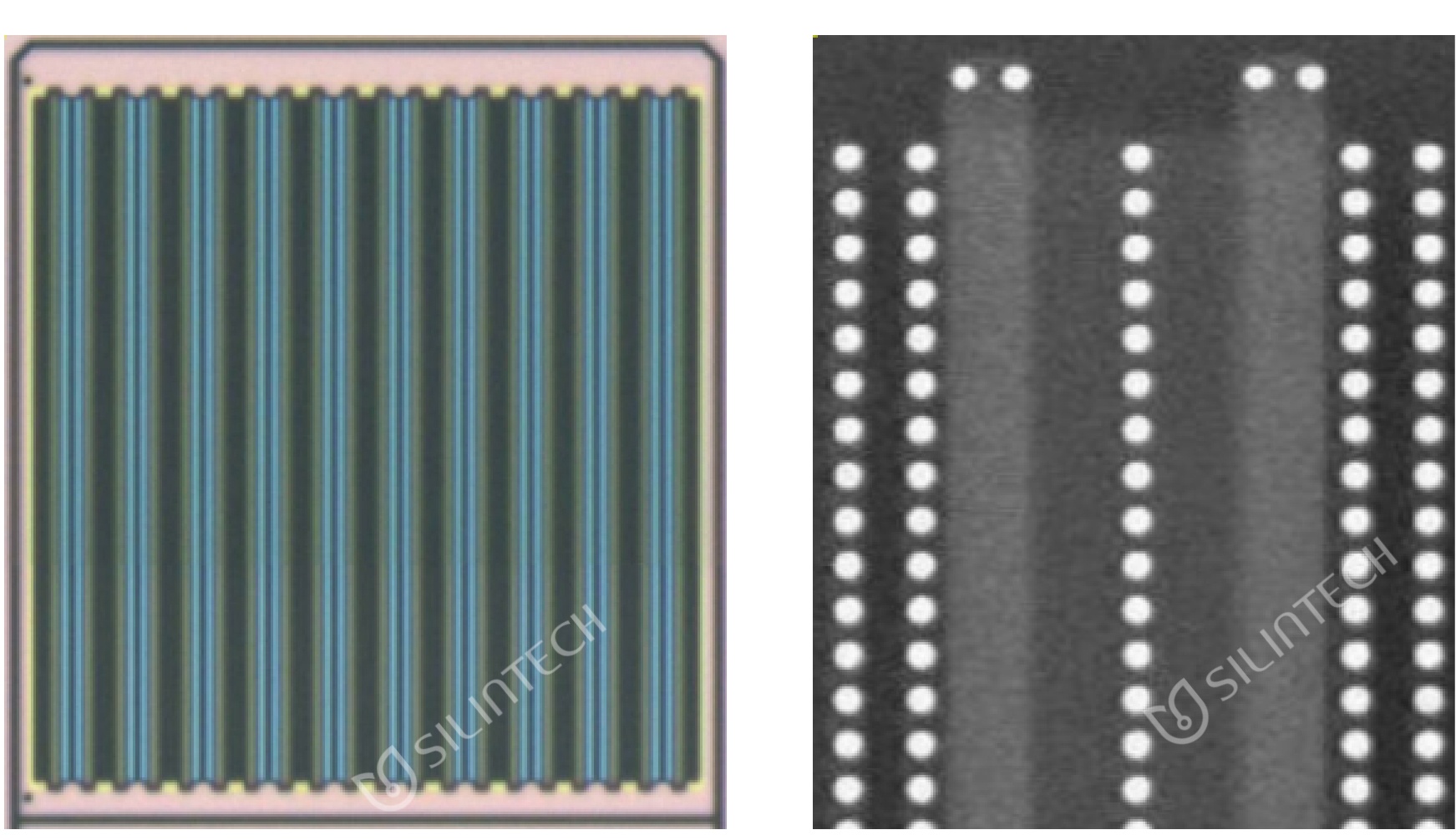
N-type drain extended high-voltage MOS transistor in the balancing module
P-type lateral diffusion power high-voltage MOS transistor in DC-DC module
The LDO module is internally divided into N-type lateral diffusion high-voltage MOS transistors
Performance comparison of BMS chips with completed circuit analysis by Silintech Inc:
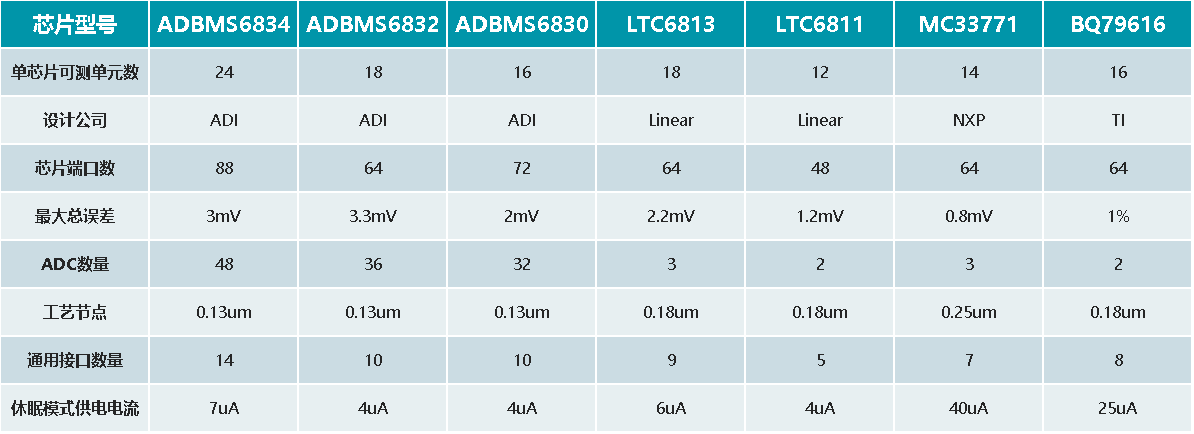
The data in the table is provided based on the chip manual
If you need to learn more detailed technical information or have consultation needs related to cooperation, please feel free to contact us at any time. We will wholeheartedly provide you with professional answers and Technical Support.