1. Project Introduction
1.1 Description
RDA5870P integrates industry-lead Bluetooth and FM radio tuner into one chip and is optimized for mobile applications. Bluetooth and FM can work simultaneously and independently, with low power consumption levels target to battery powered devices. For the highest integration level, the required board space has been minimized and customer cost has been reduced. Manufacturers
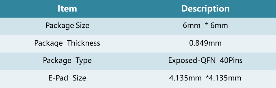
can easily and fast integrate RDA5870P on their product to enable a rapid time to market.RDA5870P uses CMOS process with a compact 6*6mm 40-pin QFN package.
1.2 Bluetooth Features
-
CMOS single-chip fully-integrated radio and baseband
-
Compliant with Bluetooth 2.1 + EDR specification
-
Bluetooth Piconet and Scatternet support
-
ARM7-based microprocessor with on-chip ROM and RAM
-
Meet class 2 and class 3 transmitting power requirement, support class1 operation with external power amplifier
-
Provides +10dbm transmitting power
-
NZIF receiver with -90dBm sensitivity
-
Battery power supply directly with internal LDO
-
Support DCXO with internal oscillator circuit
- Up-to 4Mbps high speed UART HCI support
- Support AFH
- Support 3-wire and 2-wire WIFI Co-existence handshake signals
- Low power consumption
- Minimum external component
1.3 FM Features
-
CMOS single-chip fully-integrated FM tuner
-
Low power consumption
Total current consumption lower than 20mA at
3.0V power supply -
Support worldwide frequency band
50 -115 MHz
-
Digital low-IF tuner
Image-reject down-converter
High performance A/D converter
IF selectivity performed internally
-
Fully integrated digital frequency synthesizer
Fully integrated on-chip RF and IF VCO
Fully integrated on-chip loop filter
-
Autonomous search tuning
-
Support 32.768KHz crystal oscillator
-
Digital auto gain control (AGC) Digital adaptive noise cancellation
Mono/stereo switch
Soft mute
High cut
-
Programmable de-emphasis (50/75 μs)
-
Receive signal strength indicator (RSSI)
-
Bass boost
-
Volume control
-
Line-level analog output voltage
-
32.768 KHz,26M (Reference clock)
-
I2C control bus interface
-
Directly support 32Ω resistance loading
-
Integrated LDO regulator
1.8 to 5.5 V operation voltage
1.4 Applications
-
1.8 to 5.5 V operation voltage
-
MP3,MP4 and PMP
-
PDA
-
Cordless phone
2. Chip Architectures And Functional Mudule
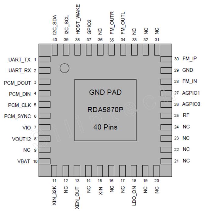
2.1 Bluetooth Chip Block Diagram
RDA5870E Bluetooth Block Diagram
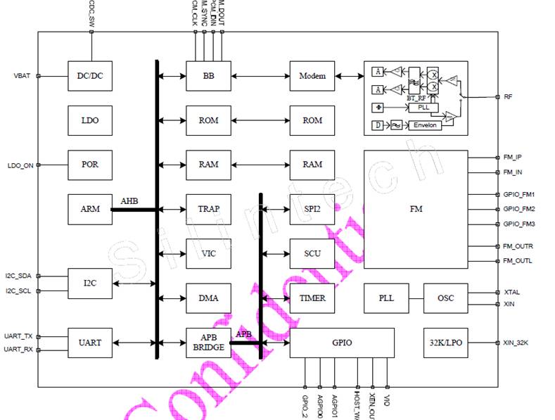
2.2 Chip Architectures
3. Chip Process And Features
3.1 Package
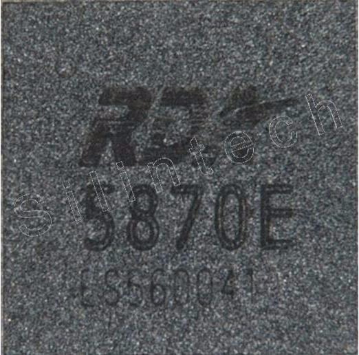
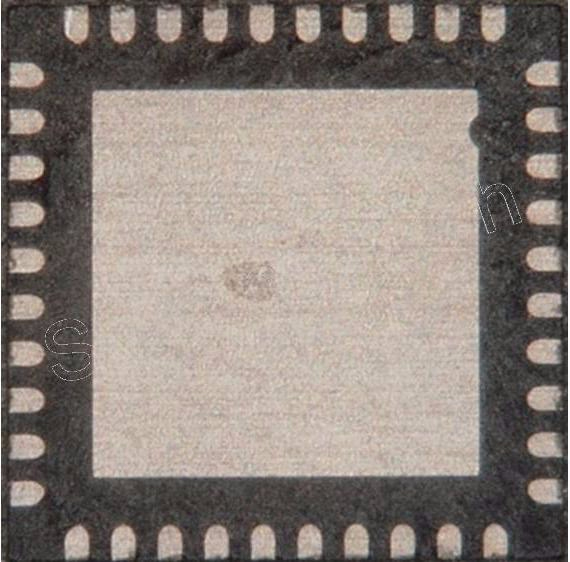
正面图 背面图
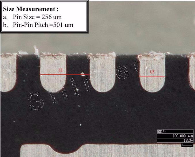
3.2 Pin size & Pin-Pin Pitch
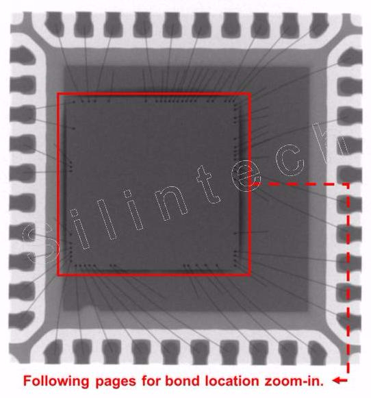
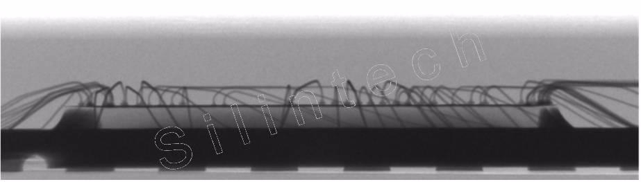
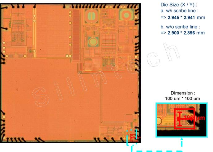
3.3 X-Ray
3.3.1 Title 90°
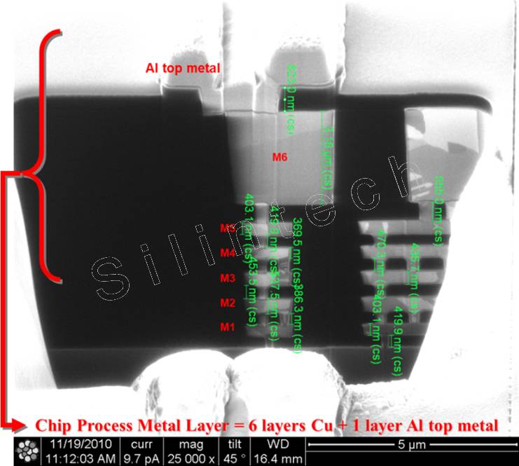
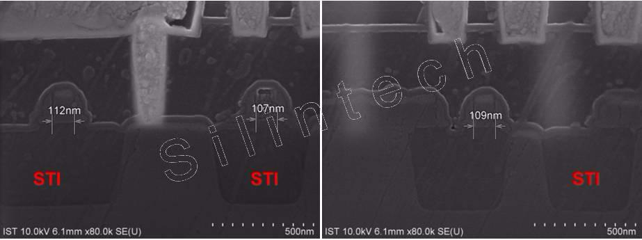
3.3.2 FIB Cross Section Image
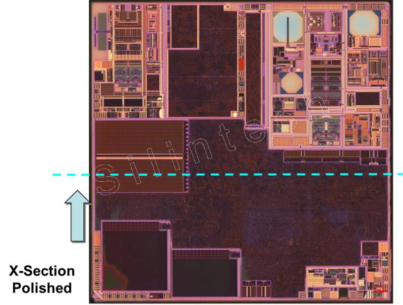
3.3.3 X-Section Line Define On Metal1
3.3.4 纵向结构分析
“ M1” Profile
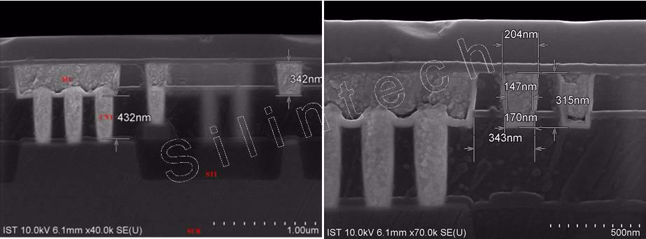
“ CNT ” Profile
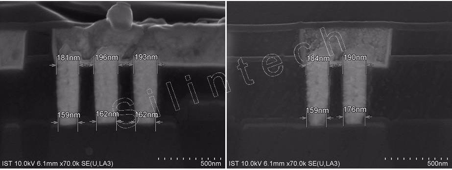
“ Poly ” Profile
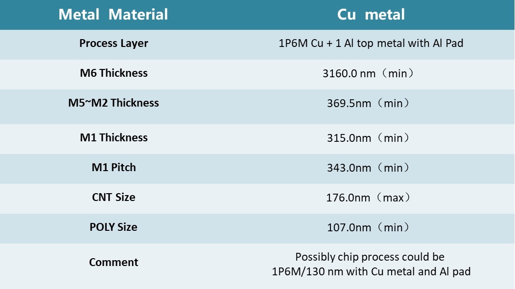
3.4 Process And Parameters
分析总结表
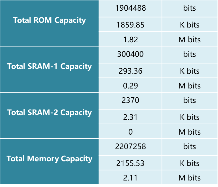
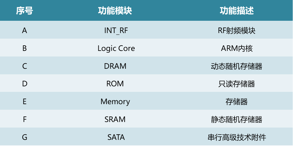
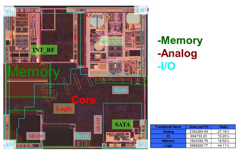
4. Memory Typle Analysis
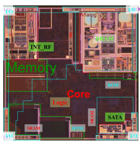
4.1 Functional Module Area Ratio
4.2 Memory Module Definition
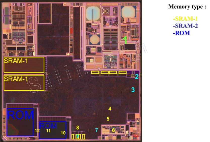
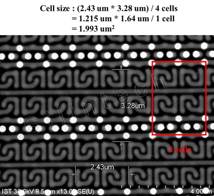
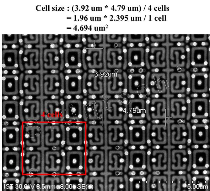
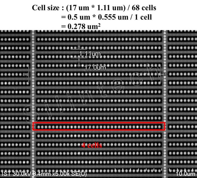
4.3 Memory Cell Analysis
4.3.1 SRAM1 On M1
4.3.2 SRAM2 On M1
4.3.3 ROM On M1
存储容量表