1. Chip Introduction
1.1 Description
The A5941 three phase motor drivers incorporate sinusoidal drive to minimize audible noise and vibration for medium The A5941 three phase motor drivers incorporate sinusoidal drive to minimize audible noise and vibration for mediumpower fans.
A sinusoidal voltage profile is applied to the windings of the motor at startup to quietly startup and gradually ramp up themotor to desired speed. The voltage profile is set to a default value that will operate for a wide range of motorcharacteristics. EEPROM can be altered to customize the startup operation if desired.
The motor speed is controlled by applying a Duty cycle command to the PWM input The PWM input is allowed to operate over a widefrequency range. If desired and analog voltage can be used to control motor speed, set via EEPROM adjustment.
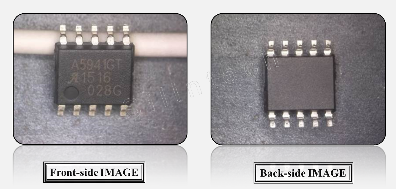
The A5941 is available in a 10L SOIC(suffix LN), and a 10 lead SOIC with exposed pad(suffix LK).
1.2 Features And Benefits
- Quiet Startup
- 180 Degree Sinusoidal Drive For Low Audible Noise
- High Efficiency Control Algorithm
- Sensorless Operation
- Wide supply voltage range
- FG Speed Output
- Lock Detection
- Overcurrent Protection
- Soft Start
- Short Circuit Protection
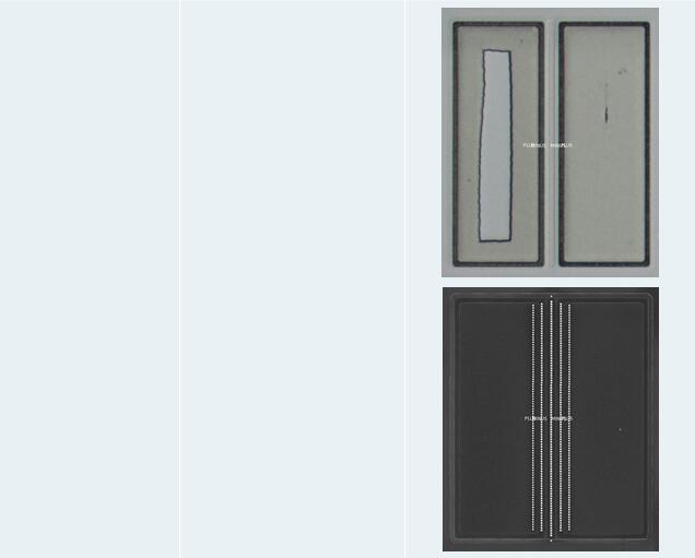
1.3 Chip Package And Markings
1.3.1 Package Markings
1.3.2 Package X-Ray
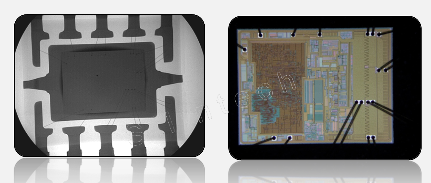
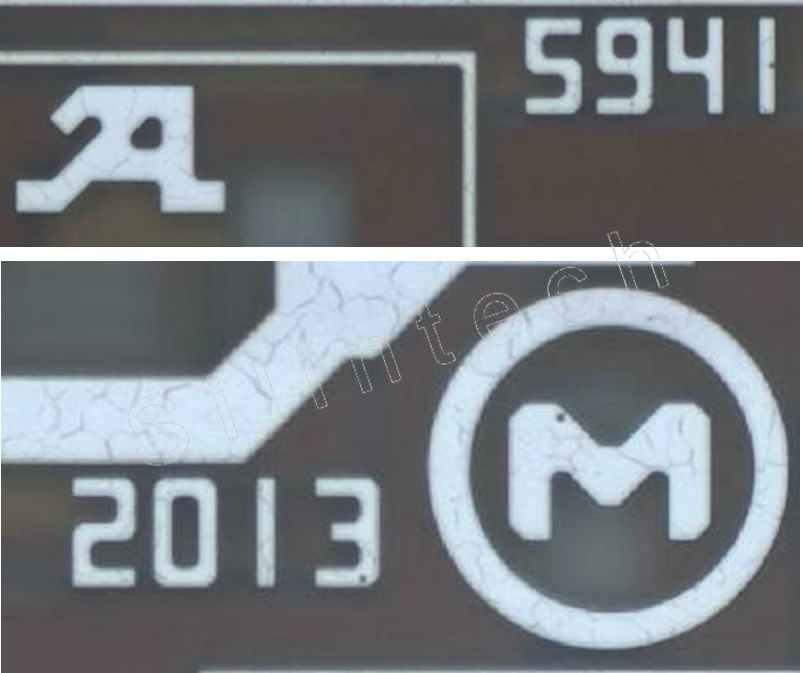
1.3.3 Die Marking
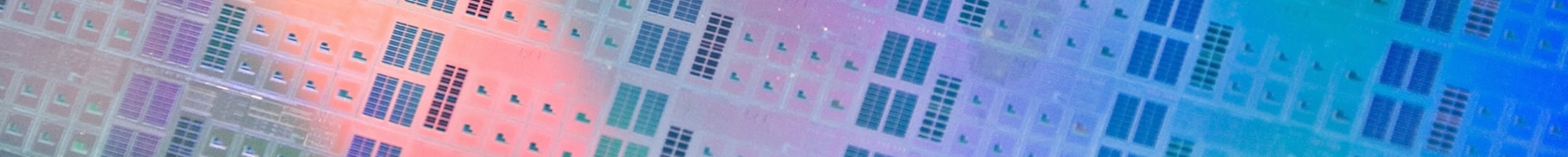
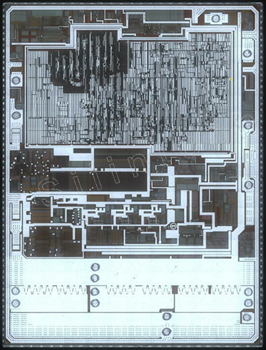
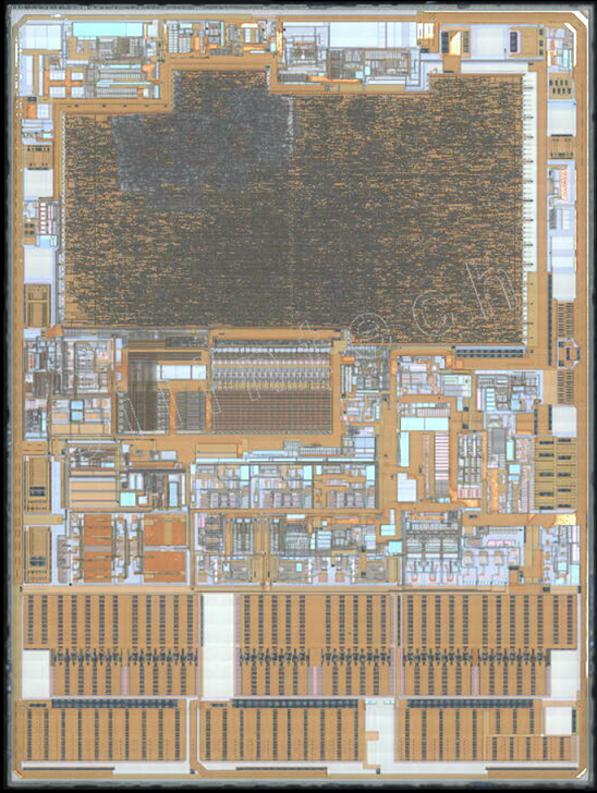
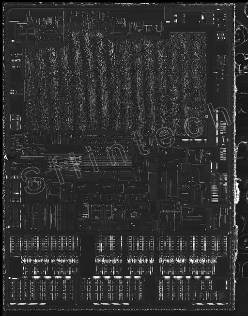
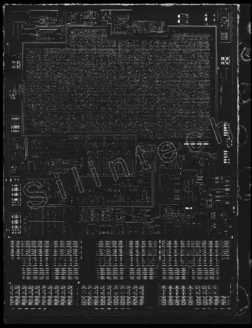
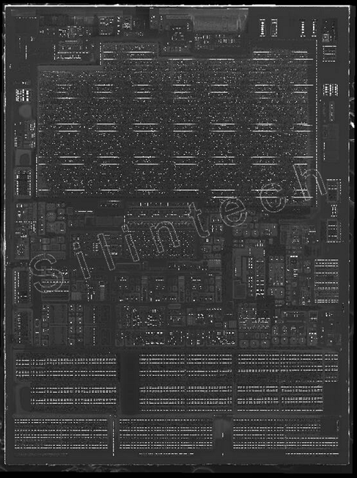
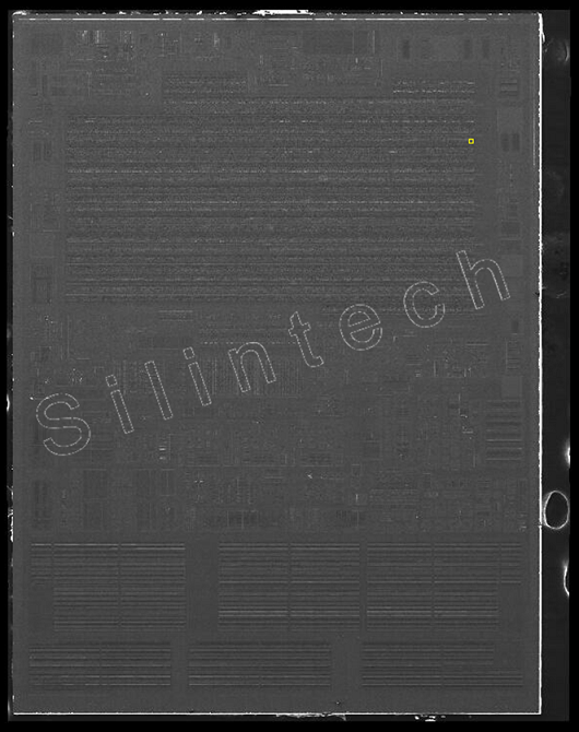
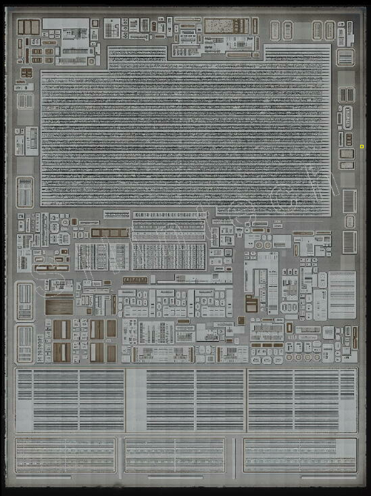
2. Die Photograph
2.1 Top Metal
2.2 Metal3
2.3 Metal2
2.4 Metal1
2.5 Poly
2.6 Diff
2.7 Stain
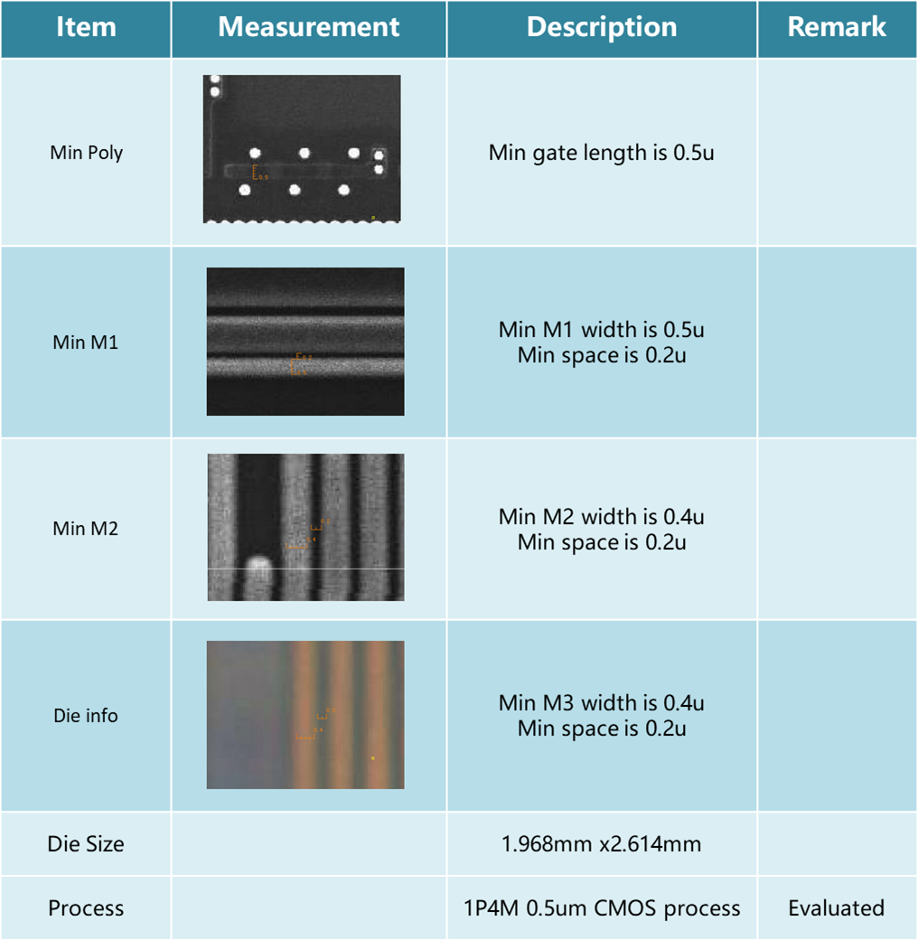
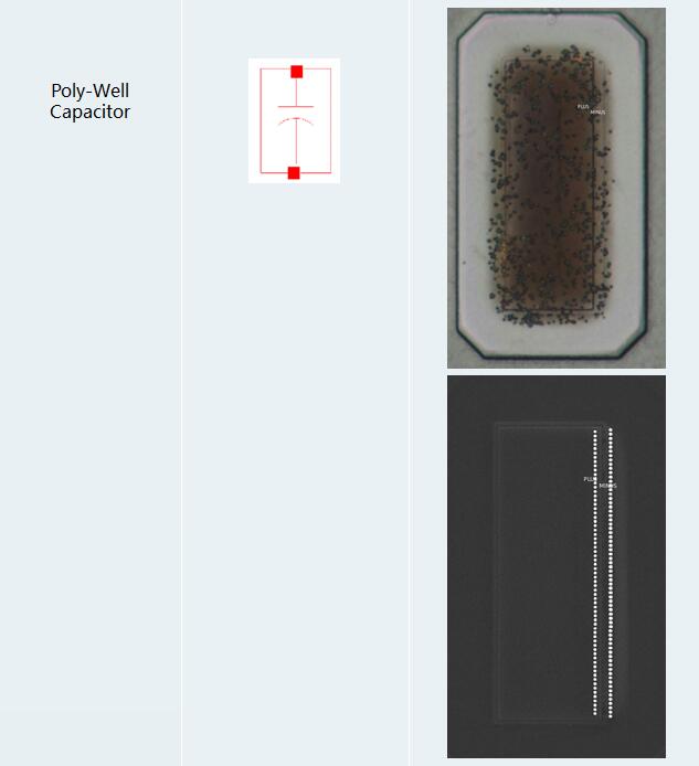
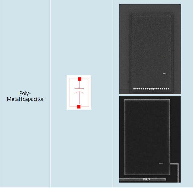
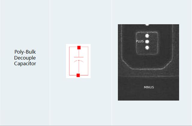
3. Die Parameter Definition
3.1 Chip Process Evaluation
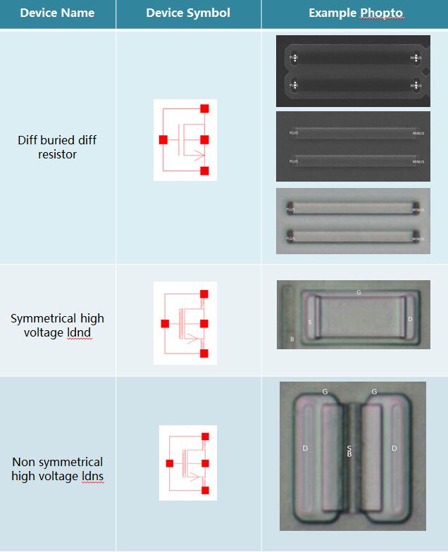
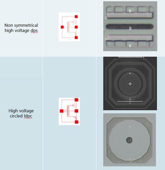
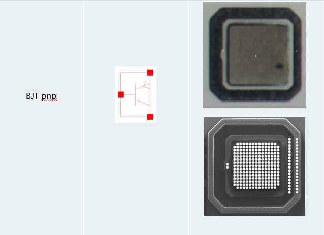
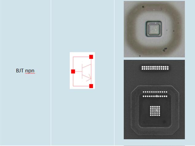
3.2 Device Summary(Exclude Normal NMOS & PMOS)
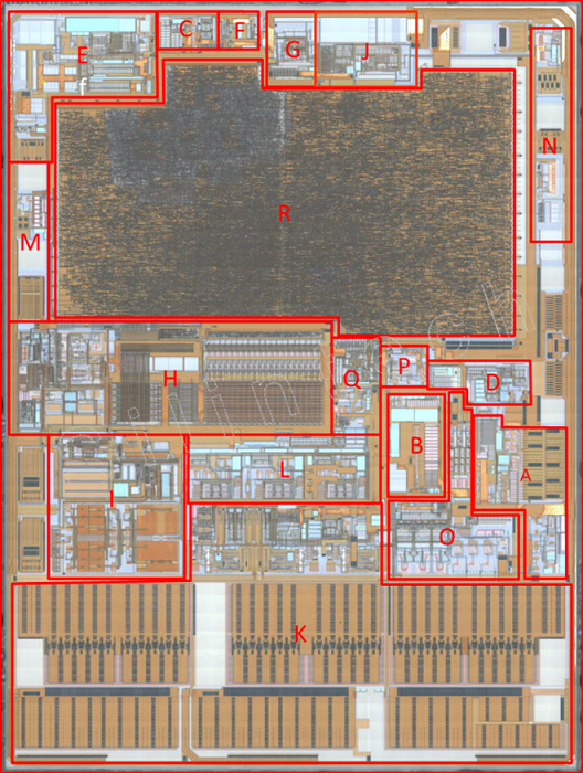
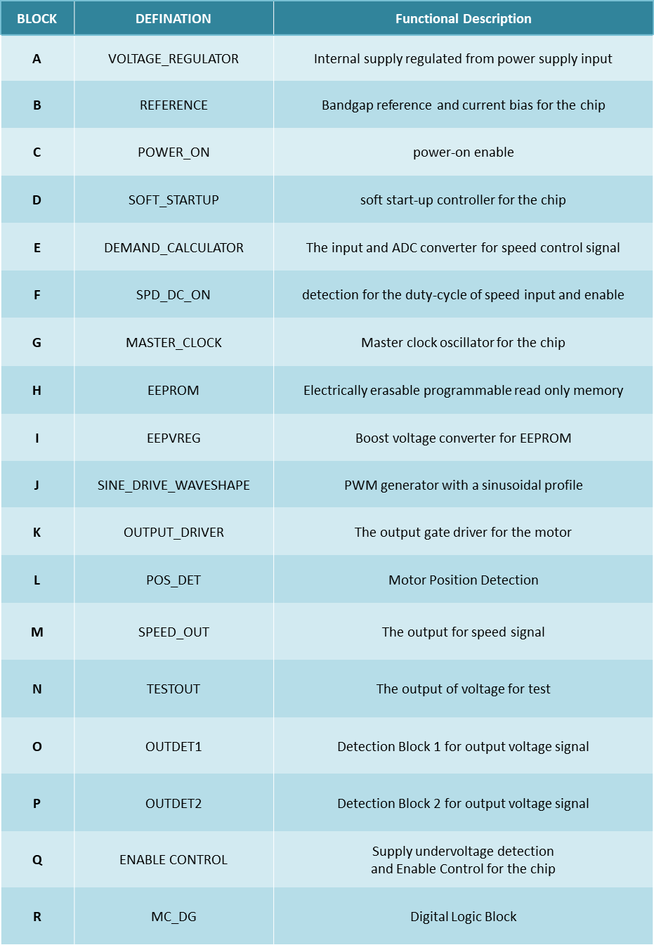
4. Layout Architecture & Overview
4.1 Chip Layout Architecture
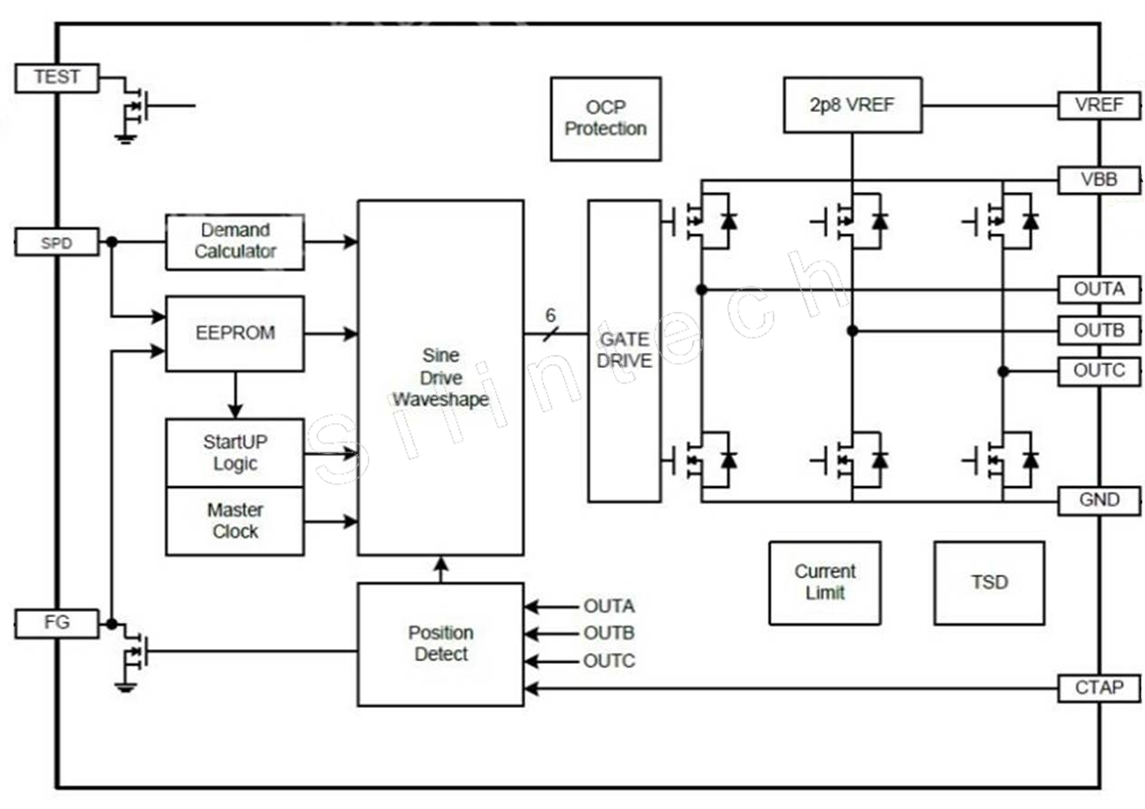
4.2 System Block Diagram
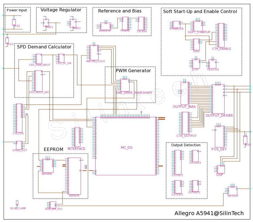
5. Reconstructed Hierarchical Schematics
▼Top Schematic
5.1 Main Subcircuit schematic
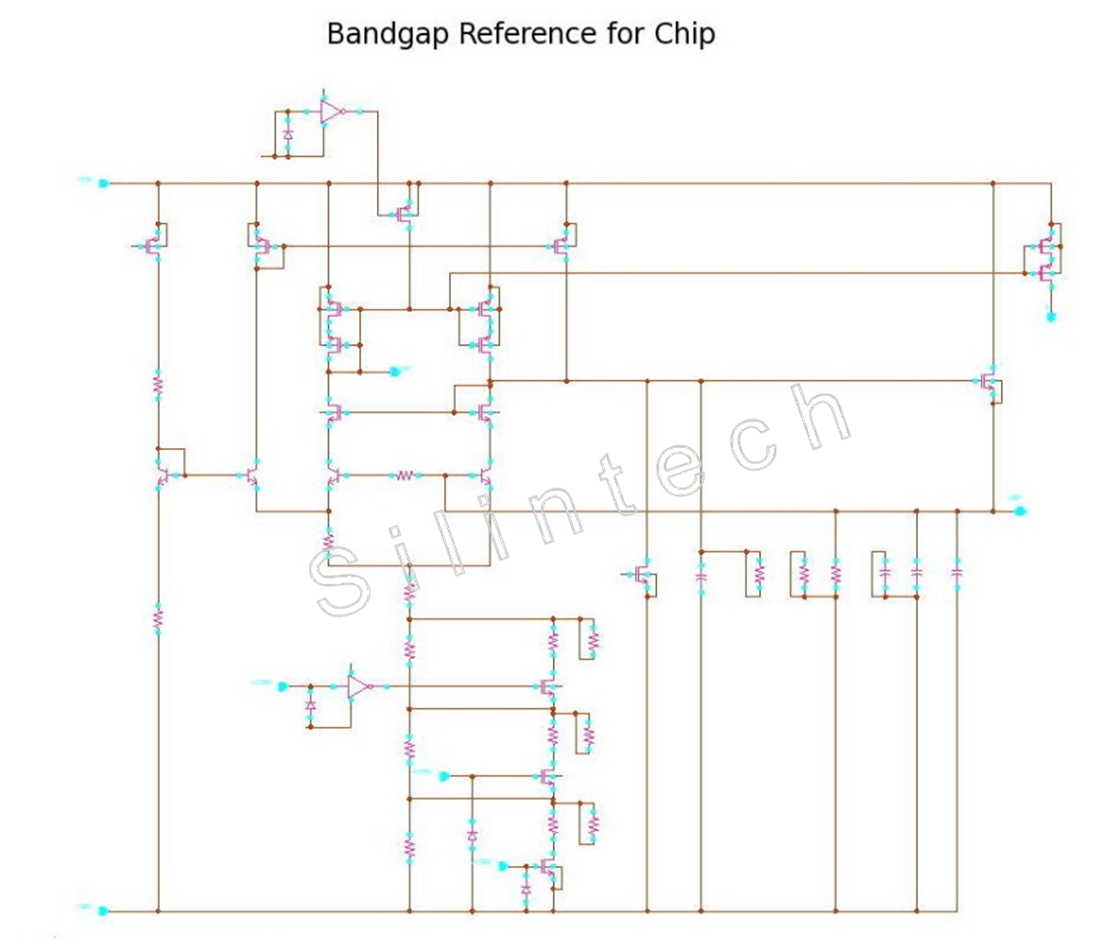
5.1.1 Bandgap Reference Circuit
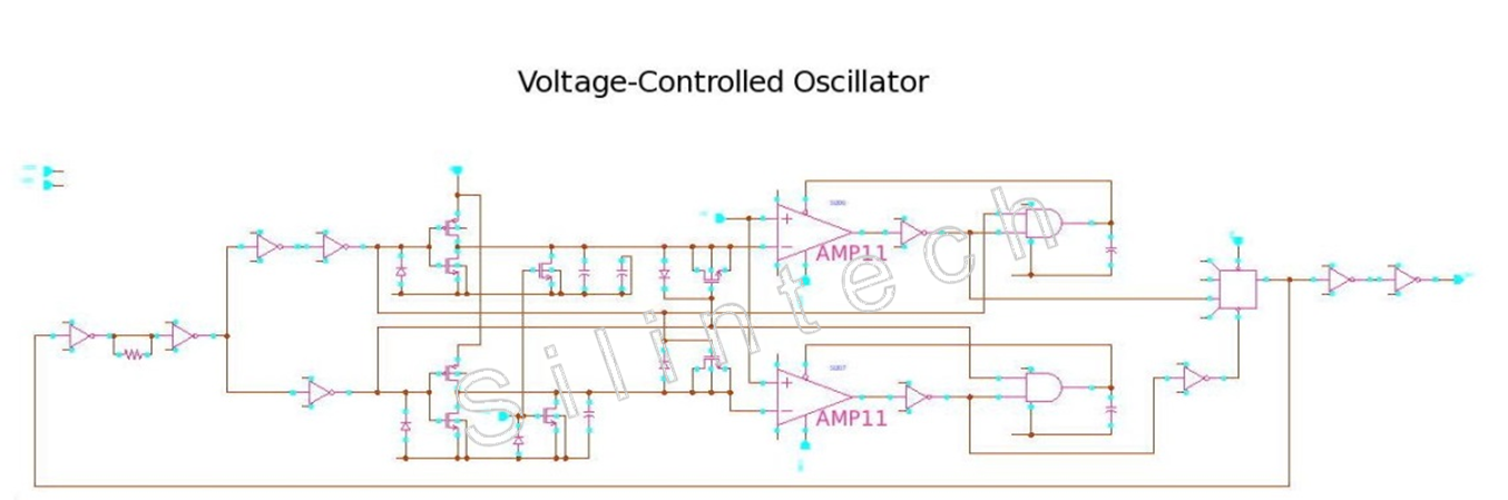
5.1.2 Main Clock Oscillator
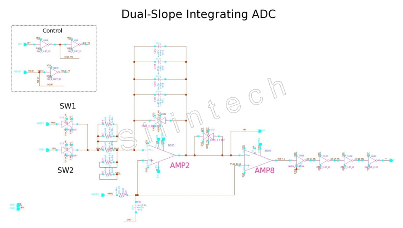
5.1.3 Speed control signal input and measurement module
The algorithm of Dual-Slope Integration is adopted for the speed input ADC. AMP2 is for integrating the input signal, and AMP8 works as a comparator. At beginning, a reference voltage is used to charge the capacitor for a fixed time, and then the input speed voltage is used to discharge the capacitor until backing to initial level, so the ratio of discharge time and charge time will reflect the input speed voltage. A high-resolution digital counter would play the role for time counting, and output the converted digital value directly. The AMP8 should be designed with very high gain so as to minimize the error.The algorithm of Dual-Slope Integration is adopted for the speed input ADC. AMP2 is for integrating the input signal, and AMP8 works as a comparator. At beginning, a reference voltage is used to charge the capacitor for a fixed time, and then the input speed voltage is used to discharge the capacitor until backing to initial level, so the ratio of discharge time and charge time will reflect the input speed voltage. A high-resolution digital counter would play the role for time counting, and output the converted digital value directly. The AMP8 should be designed with very high gain so as to minimize the error.
▼AMP8
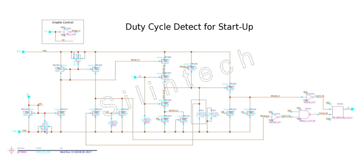
5.1.4 Duty Cycle Detect For Start-Up
The duty cycle of PWM speed signal is detected to determine if it is larger than DC_ON. When the duty cycle is too small, the integrating voltage on the capacitor is not high enough to switch on the NMOS transistor, such that there is no output signal to enable the motor drive.
5.1.5 EEPROM_CELL
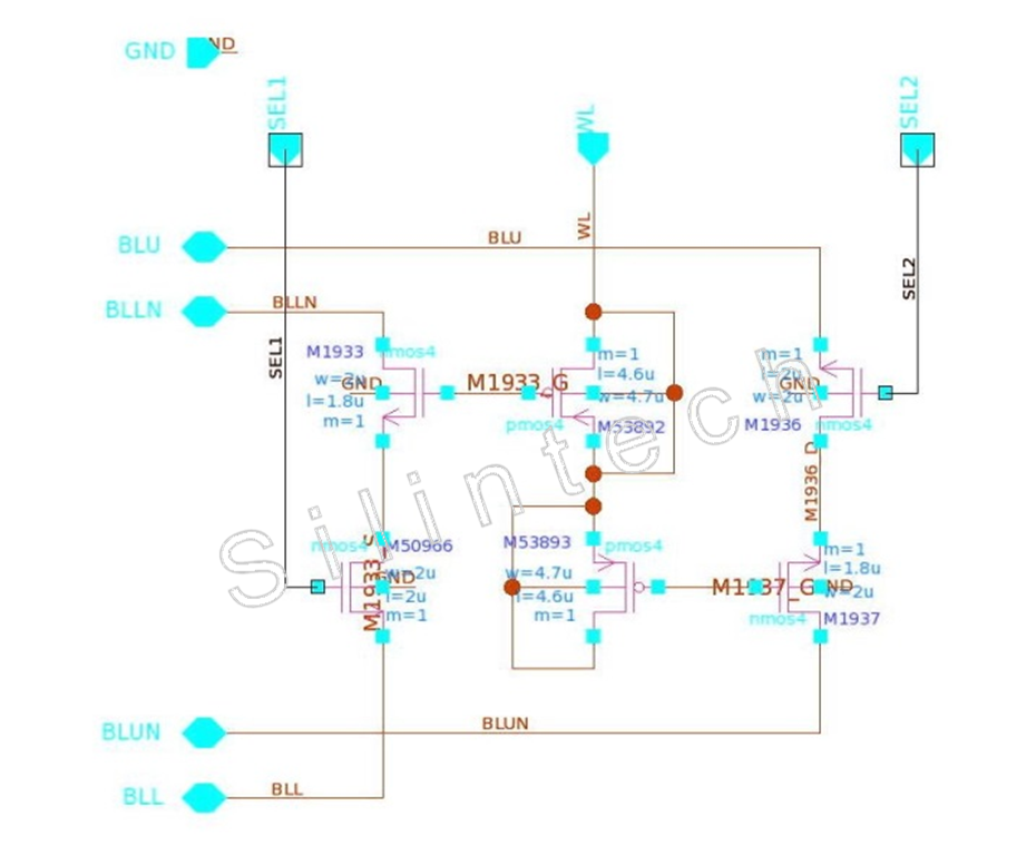
An EEPROM_CELL includes two bit-cells, and one bit-cell consists of two adjacently placed NMOS and PMOS transistors with an electrically isolated common polysilicon gate. The common gate works as a floating gate. The inversion layer under the PMOS gate and p+ diffusions works as a control node. When a positive voltage WL is applied to the p+ diffusions, the potential of the floating gate is determined by the capacitance ratio of the PMOS and NMOS gates. By selecting a proper combination of voltages of the n+ diffusion of NMOS and the p+ diffusion of PMOS, a specific EEPROM operation is achieved. Since the gate capacitance ratio of CGP (PMOS Gate capacitance) and CGN (NMOS gate capacitance) in the circuit is larger than 3, so the NMOS F/N tunneling effect is used for EEPROM write and erase mode, and the current should be small in this case. The NMOS controlled by line SEL is used to active the bit-cell, and BL line is for reading.
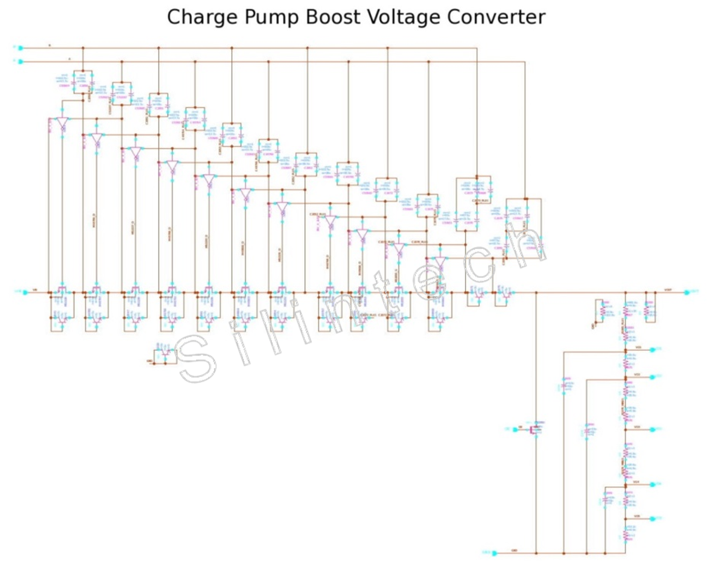
5.1.6 BOOST_CONVERTER
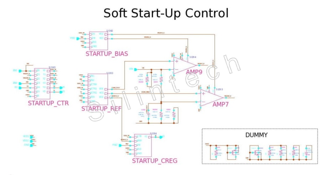
5.1.7 Soft Start-Up Control
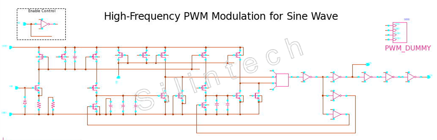
5.1.8 SINEWAVE_GEN
▼SINEWAVE_GEN Block
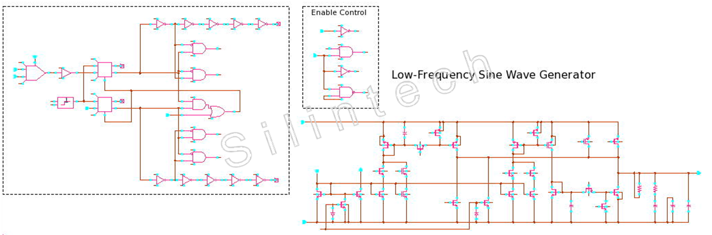
▼SINEWAVE_MOD Block
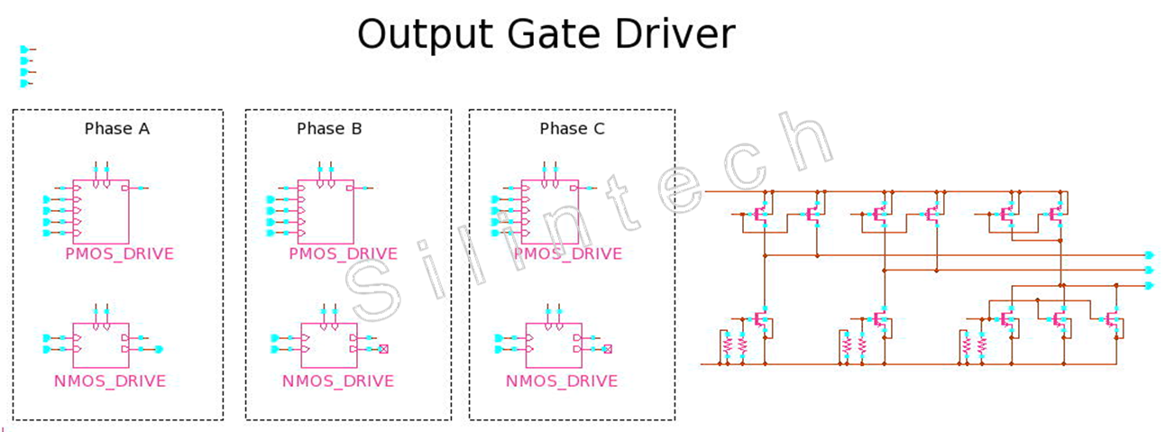
5.1.9 Output Gate Driver
5.1.10 Motor Position Detection (POS_DET)
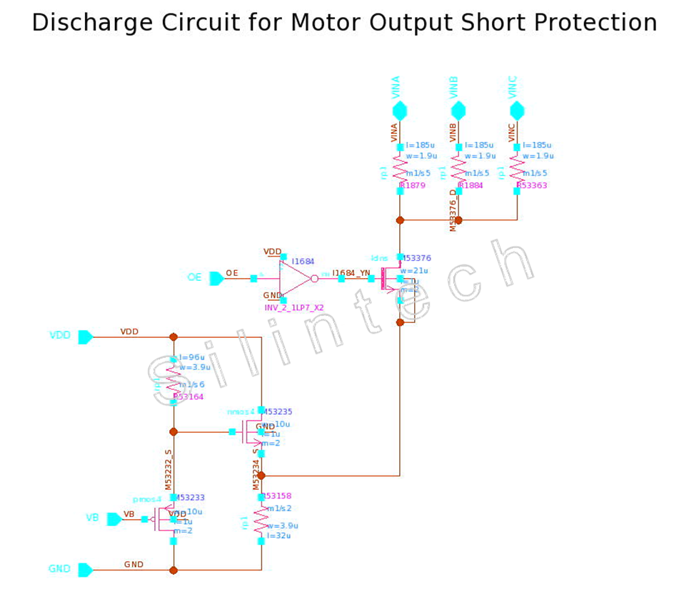
5.1.11 OSP
When the outputs of three phase motor driver connect with balanced three phase loads, the common terminal of loads is the virtually grounded. Once two outputs short connected, the voltage level at common terminal will increase greatly, such that the circuit below will work as the discharge channel to prevent the motor windings from over temperature.
6. Table Of Content
5.1 Voltage Regulator
5.1.1 VREG1
5.1.1.1 VREG_BIAS
5.1.1.2 AMP6
5.1.2 VREG2
5.2 Reference and Bias
5.2.1 BANDGAP
5.2.2 PRIBIAS
5.2.3 SECBIAS
5.3 MASTER_CLOCK
5.3.1 MC_VCO
5.3.1.1 AMP11
5.3.2 MC_BIAS
5.3.3 MC_ENABLE
5.3.4 MC_DELAY
5.4 Soft Start-Up and Enable Control
5.4.1 POWER_ON
5.4.2 SOFT_STARTUP
5.4.2.1 AMP9
5.4.2.2 AMP7
5.4.2.3 STARTUP_BIAS
5.4.2.4 STARTUP_REF
5.4.2.5 STARTUP_CTR
5.4.2.6 STARTUP_CREG
5.4.2.6.1 AMP5
5.4.3 CTR_ENABLE
5.5 SPD Demand Calculator
5.5.1 SPD_PWM_INPUT
5.5.1.1 SPD_PWM_CONV
5.5.1.2 SPD_PWM_LPF
5.5.2 SPD_INPUT_ADC
5.5.2.1 SPD_BIAS
5.5.2.2 SPD_VREF
5.5.2.3 ANALOG_INPUT
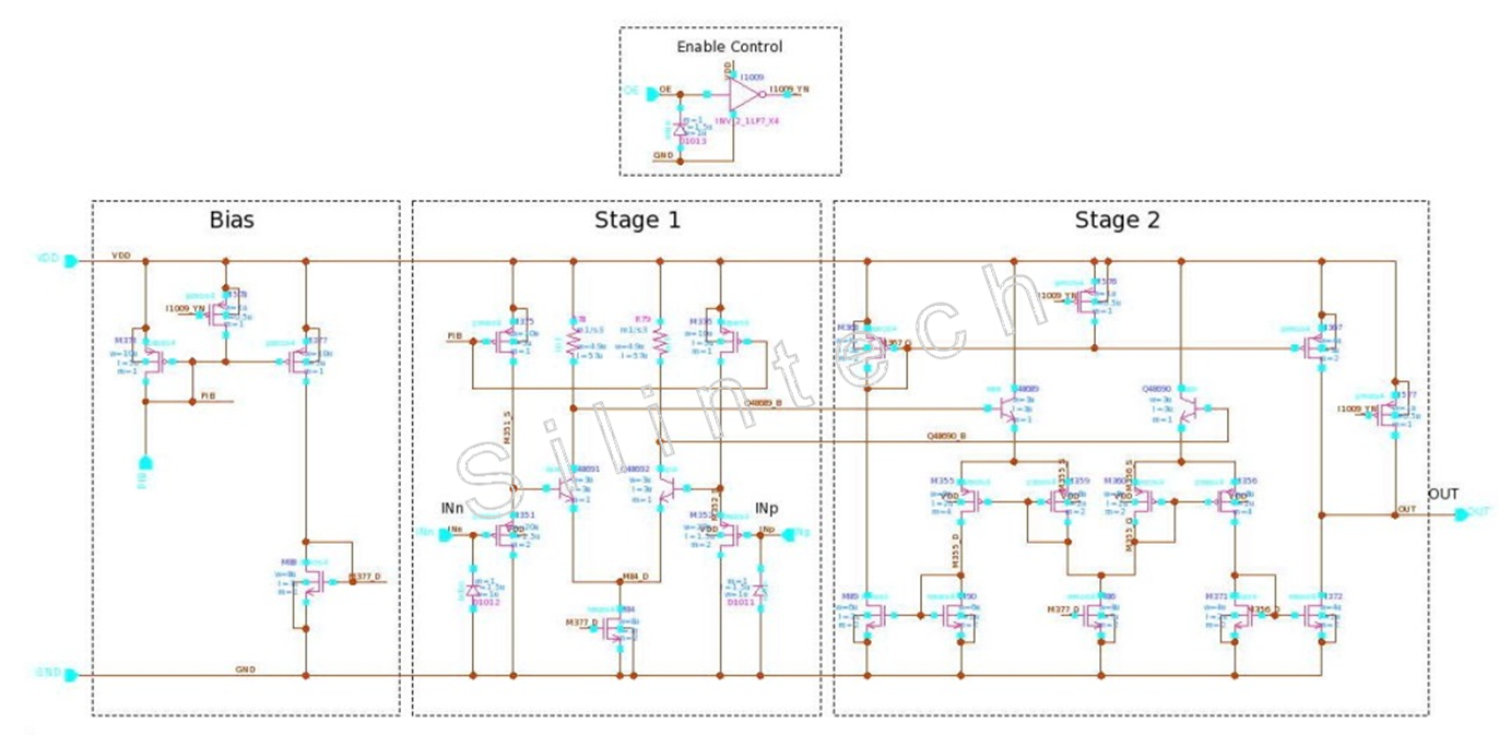
5.5.2.3.1 AMP4
5.5.2.4 SPD_ADC
5.5.2.4.1 AMP2
5.5.2.4.2 AMP8
5.5.2.5 TESTO2
5.5.3 SPD_DC_ON
5.5.4 CTR_SPD
5.6 SPEED_OUT
5.7 EEPROM BLOCK
5.7.1 EEPROM
5.7.1.1 REFERENCE
5.7.1.1.1 EEPROM_PG_REF
5.7.1.1.1.1 EEPROM_PWR_REF
5.7.1.1.1.2 EEPROM_GND_REF
5.7.1.1.1.3 EEPROM_VREF3
5.7.1.1.2 EEPROM_REF
5.7.1.1.2.1 EEPROM_BIAS
5.7.1.1.2.2 EEPROM_VREF1
5.7.1.1.2.2.1 AMP1
5.7.1.1.2.3 EEPROM_VREF2
5.7.1.1.2.4 EEPROM_VB_MUX
5.7.1.2 EEPROM_CELL_ARRAY
5.7.1.2.1 EEPROM_CELL
5.7.1.3 EEPROM_COLUMN_CTR
5.7.1.3.1 EEPROM_COLUMN_CTR1
5.7.1.4 EEPROM_COLSEL_DEC
5.7.1.5 EEPROM_VWL
5.7.1.5.1 EEPROM_VREF4
5.7.1.6 EEPROM_WR_CONTROL
5.7.1.6.1 EEPROM_WR_CTR_CELL
5.7.1.7 EEPROM_ROWSEL
5.7.1.8 EEPROM_DATAOUT
5.7.1.9 EEPROM_CTR_DEC
5.7.1.10 EEPROM_DUMMY
5.7.2 EEPVREG
5.7.2.1 EEPVREG_BIAS2
5.7.2.2 EEPVREG_DAC
5.7.2.2.1 AMP14
5.7.2.3 AMP15
5.7.2.4 EEPVREG_CTR
5.7.2.5 EEPVREG_DDRIVER
5.7.2.6 BOOST_CONVERTER
5.7.2.7 EEPVREG_LEVEL_DET
5.7.2.7.1 EEPVREG_BIAS1
5.7.2.7.2 AMP13
5.7.2.8 EEPVREG_AMP_CTR
5.7.2.9 TESTO3
5.8 SINE_DRIVE_WAVESHAPE
5.8.1 SINEWAVE_GEN
5.8.2 SINEWAVE_MOD
5.8.3 FREQ_DIVIDER
5.8.2.1 PWM DUMMY
5.9 OUTPUT
5.9.1 OUTPUT_BIAS
5.9.2 CTR_OUTPUT
5.9.3 OUTPUT_DRIVER
5.9.3.1 PMOS_DRIVE
5.9.3.1.1 PDRIVE_VREG
5.9.3.1.2 AMP17
5.9.3.2 NMOS_DRIVE
5.10 Motor Position Detection (POS_DET)
5.10.1 POS_BIAS
5.10.2 POS_DETCELL
5.10.2.1 POS_VREG
5.10.3 AMP10
5.11 Output Detection
5.12 TESTOUT
5.13 BIAS_EEP_TSO
5.14 Protection Circuits
5.14.1 UVLO
5.14.2 OTP
5.14.2.1 OTP_BIAS
5.14.2.2 AMP16
5.14.2.3 TESTO1
5.14.3 OSP
5.15 INTERFACE
5.15.1 INTF_BIAS
5.15.2 BUFFER
5.16 PAD ESD
5.16.1 ESD1
5.16.2 ESD2
5.16.3 ESD3
5.17 Basic Digital Cell
5.17.1 AND2B1_2M2_2LP7
5.17.2 AND2_2M2_1P8
5.17.3 AND2_2M2_2LP7
5.17.4 AND2_5_2P5_L1P5_M2
5.17.5 AND2_5_2P5_L1P5_M2_X1
5.17.6 AND_2M2_1LP7
5.17.7 AO21_2M2_2LP7
5.17.8 AOI22_2M2_1P8
5.17.9 BUFX2_2M2_2LP7
5.17.10 BUFX2_2M4_1P8M2
5.17.11 BUFX2_2M4_2LP7M2
5.17.12 BUFX2_2M8_2LP7M4
5.17.13 BUFX2_2_1LP7
5.17.14 CMOS_10_10_LP8
5.17.15 CMOS_2M2_2LP7
5.17.16 CMOS_2_2LP7
5.17.17 CMOS_2_2LP7_M2
5.17.18 CMOS_2_2_M2
5.17.19 CMOS_3_3M2_LP7
5.17.20 CMOS_3_3_LP7
5.17.21 CMOS_4_2
5.17.22 CMOS_5_2LP7
5.17.23 CMOS_5_5_LP7
5.17.24 DFFR_2M2_2LP7
5.17.25 DLATCH_2M2_2LP7
5.17.26 DLATCH_2M2_2LP7_X1
5.17.27 DLATCH_5L1P5_4L2
5.17.28 INVBN_2_1LP7M4
5.17.29 INV_1M2_1LP7
5.17.30 INV_1_1LP7
5.17.31 INV_2M16_1P8M8
5.17.32 INV_2M16_2LP7M8
5.17.33 INV_2M2_1LP7
5.17.34 INV_2M2_1P8
5.17.35 INV_2M2_2LP7
5.17.36 INV_2M4_1P8M2
5.17.37 INV_2M4_2LP7M2
5.17.38 INV_2M8_2LP7M4
5.17.39 INV_2_1LP6
5.17.40 INV_2_1LP7
5.17.41 INV_2_1LP8
5.17.42 INV_2_1LP7_M2
5.17.43 INV_2_1_LP7
5.17.44 INV_2_P9
5.17.45 INV_3M2_3_L1P2
5.17.46 INV_4M2_4LP7
5.17.47 INV_4_2LP7
5.17.48 INV_5L1P5_4L2
5.17.49 INV_P7_1_LP7
5.17.50 MUX21N_2M2_1P8
5.17.51 MUX21_2M2_1P8
5.17.52 MUX21_2M2_2LP7
5.17.53 NAND2B1_2_2LP7
5.17.54 NAND2_2_1P8
5.17.55 NAND2_2_2LP7
5.17.56 NAND2_2_2LP7_M2
5.17.57 NOR2_2M2_1P2
5.17.58 NOR2_2M2_1P5LP7_X1
5.17.59 NOR2_2M2_1P5LP7
5.17.60 NOR2_2M4_1P8
5.17.61 NOR3_2M2_1P2
5.17.62 NOR3_2P5M2_1P5LP7
5.17.63 SMITINV_2_1LP7
5.17.64 SMITINV_2_1LP7_X1
5.17.65 OAI21_2M2_2LP7
5.17.66 OAI21_2M2_1P8
5.17.67 OR2_2M2_2LP7
5.17.68 OR2_2M3_1P8
5.17.69 OR3B3_2M2_2LP7
5.17.70 OR3_2M2_1P8
5.17.71 OR3_2M2_2LP7
5.17.72 RS_LATCH_2M2_1P5LP7
5.17.73 RS_LATCH_2_2LP7
5.17.74 RS_LATCH_2_1P8
5.17.75 RS_LATCH_2_2LP7_X1
5.17.76 RS_LATCH_5L1P5_10L2
5.17.77 SMITBUF_3P2L1P2M2_2P5L1
5.17.78 TIEHI_2_1LP7
5.17.79 TIELO_2_P9
5.17.80 XNOR2_2M2_2LP7
5.17.81 XOR2_2M2_1P8
5.18 VSUB_CLAMP