Introduction:When BYD claimed to be able to complete 400 kilometers of range refueling in 5 minutes, people were amazed by the feat of "oil and electricity at the same speed" rewriting the history of electric vehicles. But few people have noticed that behind this high-voltage revolution is the ultimate test of battery management systems (BMS): the safety management of batteries on the 1000V voltage platform, even a small voltage deviation of a single cell can trigger a chain reaction. This leads to the core of BMS: the vehicle grade battery monitoring chip.
High precision monitoring chips represented by LTC6813 and ADBMS6830, like the "nerve endings" of a battery pack, capture the voltage, temperature, and health status of each battery cell in real time. In BYD's global kilovolt architecture, these chips are connected in series with hundreds of energy-saving chips through cascade technology, with a measurement accuracy of ± 2mV, to build a strong safety line for megawatt flash charging.

Let's take LTC6811, LTC6813, and ADBMS6830 as examples to see the true face of these chips.
This series of chips was originally developed by Linear Technology Corporation. After being acquired by Analog Device Inc in 2016, the subsequent development and production of the LTC6813 series were led by ADI. LTC6813 also transformed into ADBMS1818, becoming a new milestone in the series.
The following is the basic information of each chip:
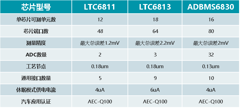
Note: The data in the table is based on the chip manual provided
From the data in the table alone, LTC6813 has 50% more measurable units than LTC6811, corresponding to an increase in port count, total error, ADC count, general interface count, and sleep mode power supply current. However, there has been no change in process nodes and transmission rates, indicating that the upgrade of this generation is mainly due to stack volume; Let's take a look at ADBMS6830 again. Firstly, there has been an improvement in the manufacturing process, with two fewer measurable units compared to LTC6813. However, the number of ports and ADCs has increased significantly, and the transmission rate has also doubled. The power supply current in sleep mode has decreased, indicating significant structural changes. Next, let's further explore their differences.
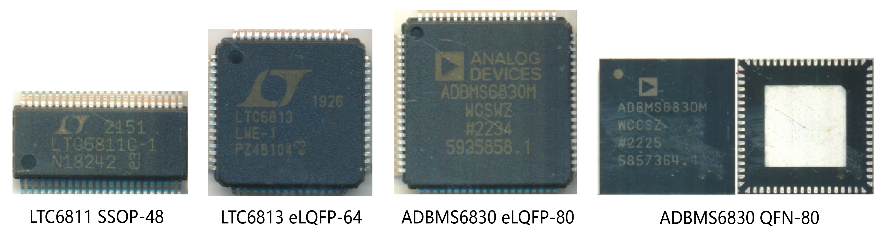
Firstly, let's take a look at the packaging of these three chips: LTC6811 adopts a 48 pin SSOP package, which has a smaller size and mainly relies on pin heat dissipation; The LTC6813 has been upgraded to a 64 pin eLQFP package with a metal pad at the bottom center, further improving heat dissipation efficiency; Under further development by ADI, the ADBMS6830 has added a QFN package version in addition to the original 80 pin eLQFP package, which further reduces the chip area while also having metal pad heat dissipation.
The following are the packaging diagrams of each chip:
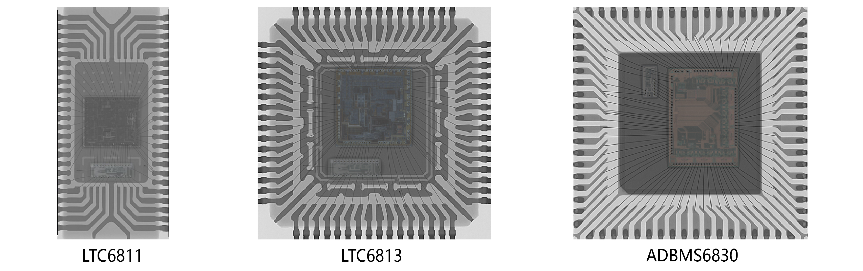
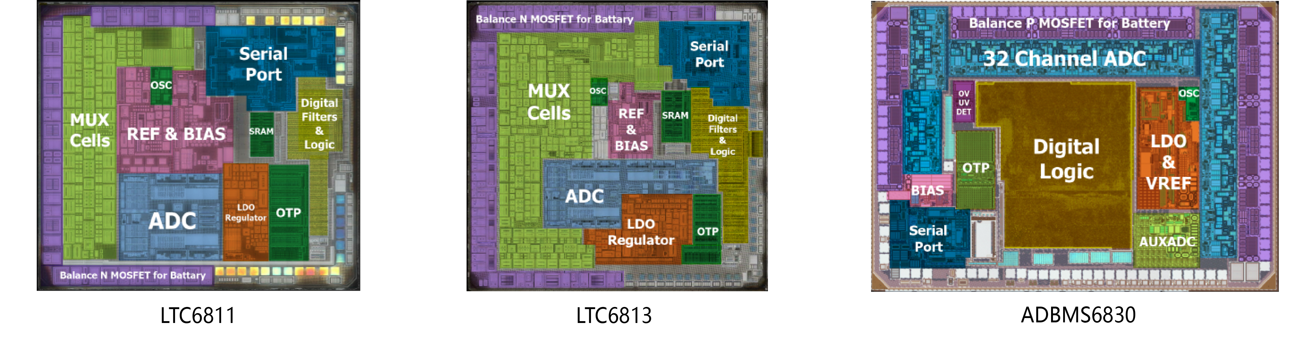
From the X-ray, it can be seen that these chips have a dual die structure inside, with the larger ones responsible for the main functions of the chips and the smaller ones serving as key pressure assistance. This dual die method has been consistently used in this series.
The following is an X-ray image:
Entering the interior of the chip, from the analyzed floorplan and top layer, it can be seen that the battery voltage to be detected in LTC6811 enters the ADC path after being selected by the MUX, and then outputs the result from the serial interface after passing through the FIR digital filter. On the basis of LTC6811, LTC6813 has upgraded the number of units, synchronously increased the number of multiple selection channels in the MUX, and added an ADC path. The main architecture remains largely unchanged as speculated.
However, ADBMS6830 made a major change to the chip architecture. Firstly, the MUX channel was removed and replaced with twice the number of ADC detection units for synchronous redundant detection of batteries. Secondly, the finite impulse response (FIR) filter was replaced with an infinite impulse response (IIR) filter, which improved computational efficiency and noise reduction effect; In addition, an additional auxiliary ADC has been designed to accurately obtain key data such as temperature, power supply voltage, and reference voltage.
The following is the floorplan:
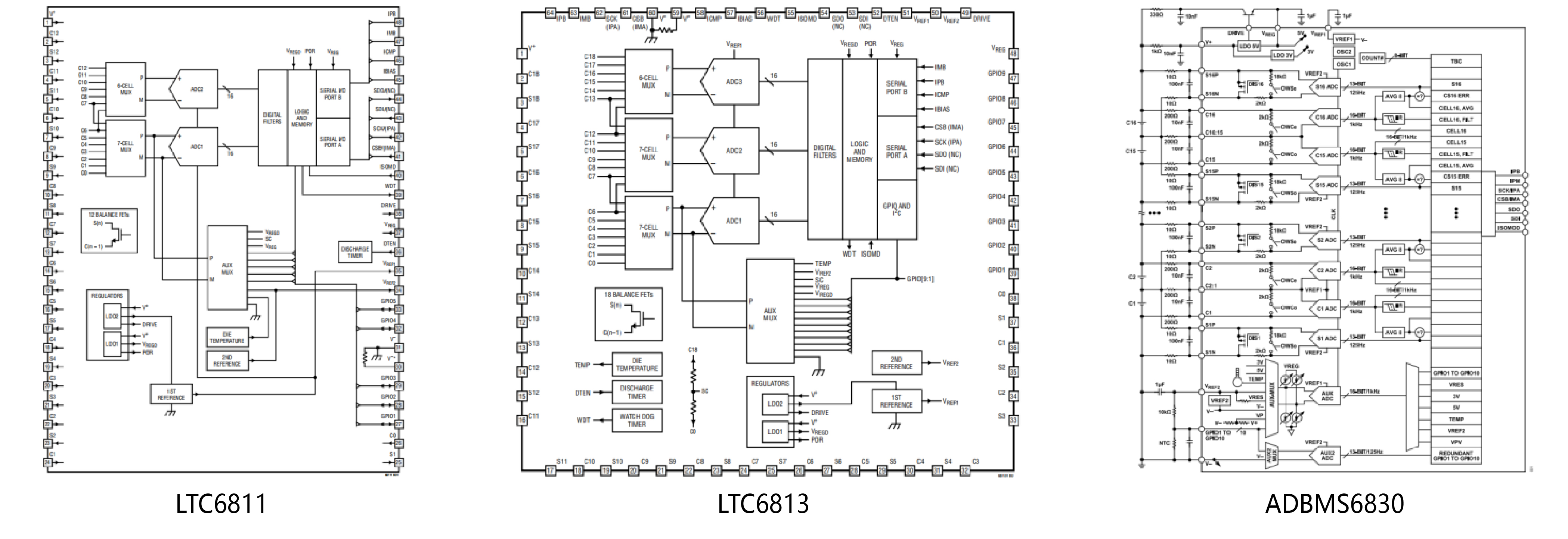
The following is the top-level schematic diagram:
The above displays the packaging design, X-ray perspective view, and internal structure analysis of this series of chips. In the next article, we will conduct in-depth analysis of this series of chips from multiple dimensions. Please stay tuned for updates.