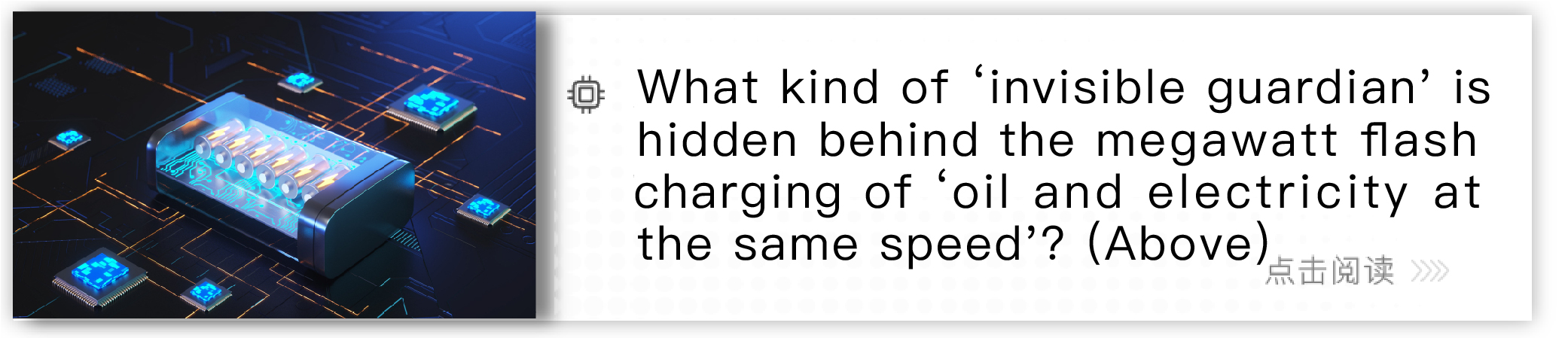
Behind the breakthrough in the megawatt flash charging technology of "oil and electricity at the same speed", there is a group of little-known "invisible guardians" - battery management chips and power control units. These precision chips constantly monitor the voltage, temperature, and charge balance of each battery in extreme environments of high temperature, high voltage, and strong electromagnetic interference, and ensure charging safety through millivolt level precision sampling technology.
In the previous content, we focused on the "external form and internal structure" of three chips, LTC6811, LTC6813, and ADBMS6830. Through packaging design analysis, X-ray perspective presentation, and internal structure disassembly, we took everyone to intuitively experience the details and ingenuity of these three chips in hardware design.
Click on the image below to review the previous content:
Today, we will further delve into this foundation - from functional feature testing to application scenario implementation, from performance parameter comparison to core technology highlight interpretation, fully unlocking the performance and value of the three chips in practical applications, and presenting a more complete technical overview for everyone.
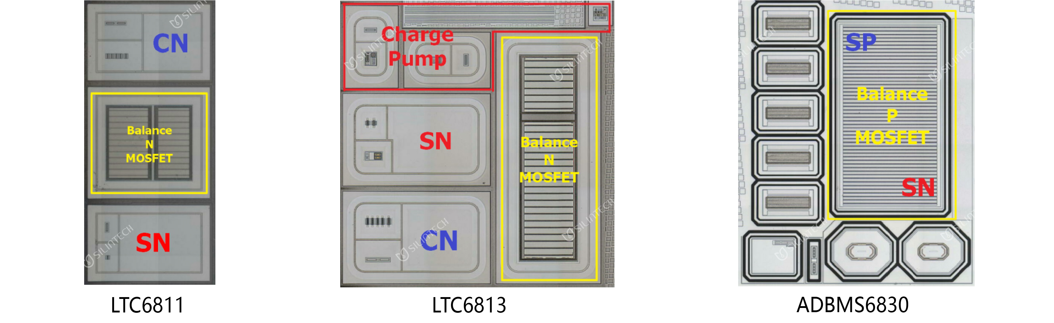
Firstly, from a technical perspective, taking the balanced switch design as an example, the LTC6811 single cell battery detection range covers 0-5V. The chip integrates balanced NMOS transistors, which can achieve a maximum balanced current of 200mA in passive balancing mode, effectively balancing the power of each battery. By increasing the number of detection units, the maximum detection voltage of a single chip in LTC6813 is increased by about 50% compared to LTC6811. A charge pump has been designed to provide higher driving voltage (as shown in the figure below), which has also increased the size of the balanced NMOS transistor. However, the overall area of the balanced module has also been nearly doubled.
The ADBMS6830 adopts a completely new process and design method. The LTC6811 and LTC6813 are measured and balanced through the battery port CN and balance port SN, while the ADBMS6830 adds an additional SP balance port for external resistors, making it easy to transfer balance heat outside the chip and improving heat dissipation performance; The internal balancing transistor has been upgraded to a PMOS transistor and replaced with a low-level driver. This not only eliminates the need for a level conversion module, but also reduces circuit complexity and layout area. In unbalanced states, parasitic diodes can naturally block leakage current and reduce static power consumption.
The following are photos of the balancing module area:
Looking down along the data path, both LTC6811/LTC6813 switch data through a six/seven select MUX channel and transmit the test data to the corresponding ADC. The 12 units of LTC6811 are matched with 2 ADCs, while the 18 units of LTC6813 correspond to 3 ADCs; The ADBMS6830 allows data to be directly transmitted to the dedicated ADC, and all ADCs work synchronously and in parallel, maximizing efficiency.
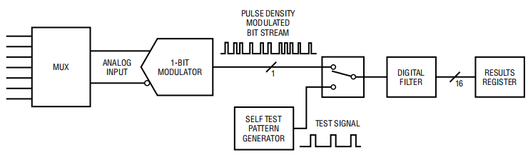
The LTC6811 and LTC6813 chips use 16 bit Sigma Delta ADCs with identical structures. The analog end adopts a one bit modulator with second-order integration, which weights and integrates the output of the previous stage and the input of the current order through a feedback path, and finally quantizes the output. This structure can provide stable frequency response, laying a solid foundation for data acquisition. More flexibly, based on different oversampling rates, the ADC is designed with 8 working modes - each mode corresponds to differentiated accuracy and timeliness, allowing users to choose as needed and adapt to more scenarios.
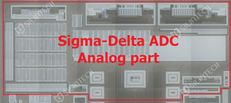
LTC6811-ADC module photo
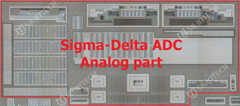
LTC6813-ADC module photo
LTC6811<C6813-ADC Structure Block Diagram (Source Chip Manual)
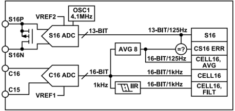
Based on the addition of an SP port as mentioned earlier, the ADBMS6830 has redesigned the ADC and adopted a dual ADC structure to accurately measure each unit (as shown in the figure below). The C-ADC is used to synchronously measure the input of the differential unit, with an input range of -2V~5.5V. It outputs 16 bit results every 1 millisecond and provides the average of the last 8 sets of data every 8 milliseconds; S-ADC is used to measure the input of the balanced differential unit, with an input range of 0-5.5V and a result output every 8 milliseconds. At the same time, S-ADC can also use C-ADC for redundant measurement of battery voltage. It is worth mentioning that the two ADCs of ADBMS6830 can reach 4MHz in continuous operation mode, which can reduce external analog filtering and produce non aliasing measurement results. Subsequently, it is further denoised through an infinite impulse response (IIR) filter.
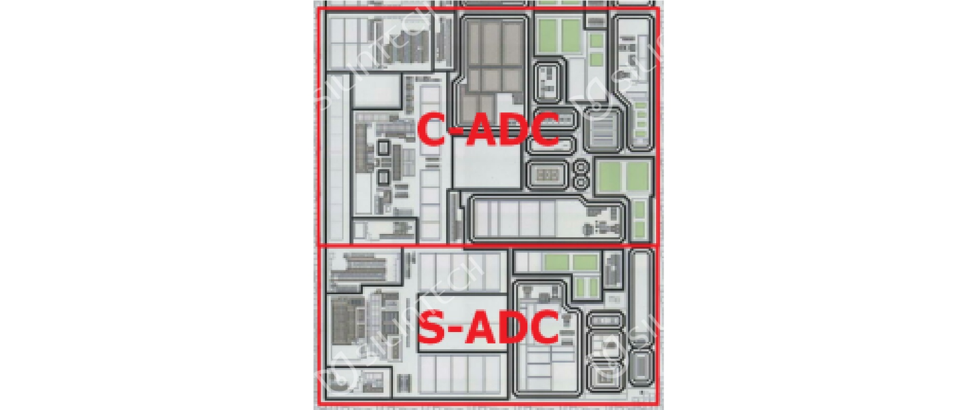
Photo of ADBMS6830-ADC module
ADBMS6830-ADC structure diagram (source chip manual)
The complete design of Sigma Delta ADC relies on digital filters. The simulation of LTC6811 and LTC6813 uses a relatively simple structure of a one bit modulator, which generates a large amount of high-frequency noise during operation. Therefore, more complex digital filters are needed to filter it out. After analysis, it was found that both chips use a third-order SINC filter as the core filtering unit. As a special type of FIR filter, the SINC filter works based on discrete time convolution operation, occupying less computing resources than traditional linear multiplication and addition FIR filters. It also has the characteristics of fast response and stability, which can effectively filter out high-frequency noise. A single SINC filter has a simple structure and average filtering effect, so it is usually composed of 3-5 cascades to achieve better filtering effect.
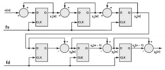
SINC3 Filter Schematic (Source Chip Manual)
For ADBMS6830, due to its inclusion of multiple ADC channels that require synchronous operations and relatively limited hardware resources, choosing an IIR filter with less multiplication and addition operations becomes a more reasonable solution. IIR filters achieve low order and efficient filtering through recursive structures, but the recursive nature may cause the poles to fall outside the unit circle, leading to system instability. It is speculated that the designer cancelled multiple operating modes of the original ADC for this consideration, in order to improve the stability of the system at a single frequency.
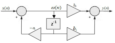 IIR Filter Schematic (Source Chip Manual)
The above is today's sharing. If you need to learn more detailed technical information or have consultation needs related to cooperation, please feel free to contact us at any time. We will wholeheartedly provide you with professional answers and Technical Support.